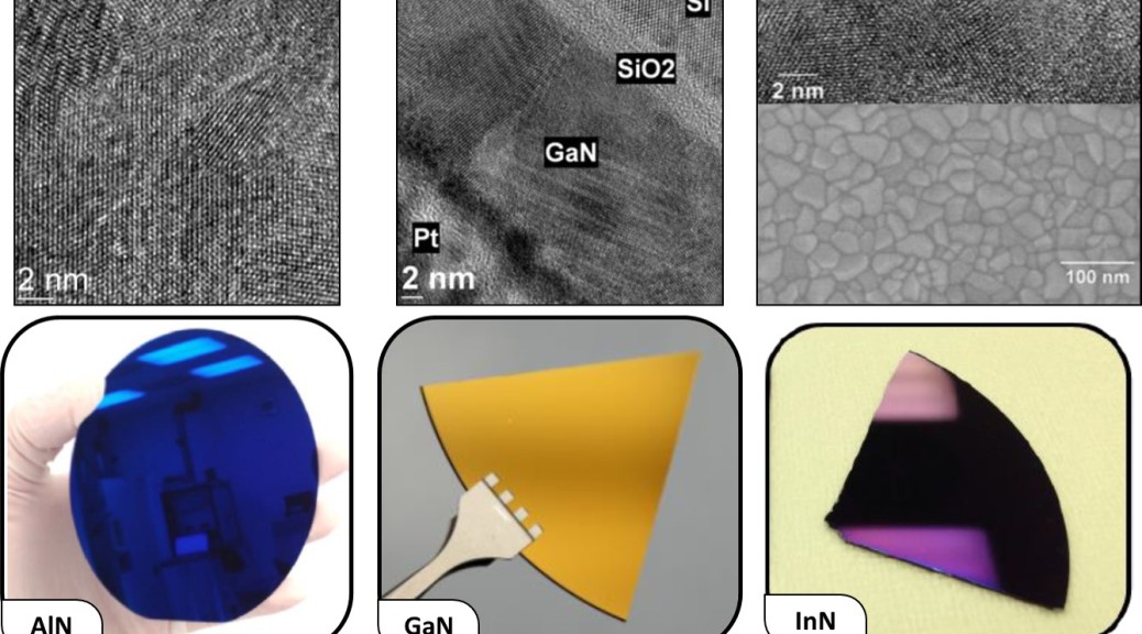
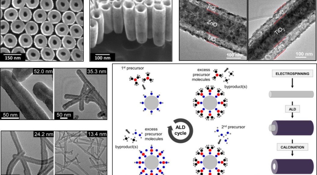
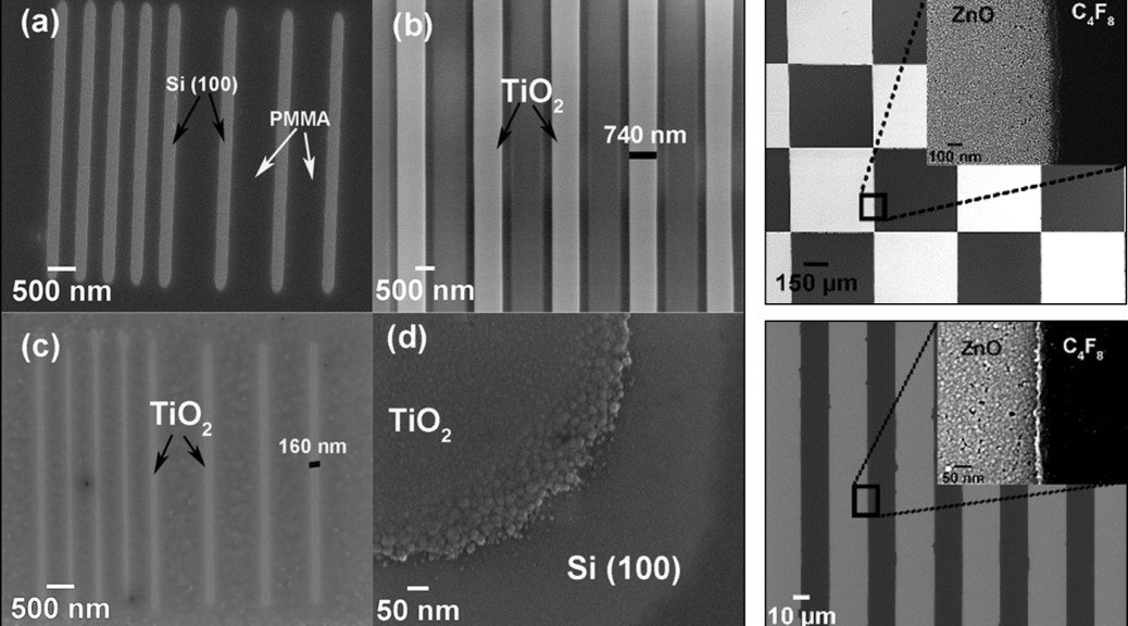
♦ We are interested in exploring functional materials processing at the atomic scale. We exploit thermal and plasma-assisted processes towards self-limiting deposition/etch of nitrides, oxides, and metals with sub-monolayer precision. Our cumulative research goal is to develop highly-selective atomic layer processes which will enable self–aligned and lithograhpy–free device fabrication with atomic resolution. ♦
Biyikli Research Group
Cover Articles
- Hollow cathode plasma assisted atomic layer deposition of crystalline AlN, GaN, and Al_x Ga_(1-x) N thin films at low temperatures
- Selective isolation of the electron or hole in photocatalysis: ZnO-TiO_2 and TiO_2-ZnO core-shell structured heterojunction nanofibers via electrospinning and atomic layer deposition
Plasma-assisted ALD of III-nitride thin films for flexible (opto)electronics
Template-assisted ALD of nanostructured oxides and nitrides for photocatalysis, photovoltaics, and energy storage
Selective atomic layer processes for self-aligned nanofabrication
ALD of metallic nanoparticle coatings of nanofibrous templates for catalysis
Characterization of mechanical properties of PA-ALD (Plasma-Assisted Atomic Layer Deposition) coated GaN thin-films
Capacitive sensor integrated MEMS Microgripper for micro and nano scale Materials Characterization
8
Core-team of BIYIKLI Group
We are interested in exploring functional materials processing at the atomic scale. We exploit thermal and plasma-assisted processes towards self-limiting deposition/etch of nitrides, oxides, and metals with sub-monolayer precision. Our cumulative research goal is to develop highly-selective atomic layer processes which will enable self–aligned and lithograhpy–free device fabrication with atomic resolution.